
Online service
Service hours: Monday to Saturday 9:00-18:00
Please choose online customer service:
Please choose online customer service:
0755-83483730 / 23823366
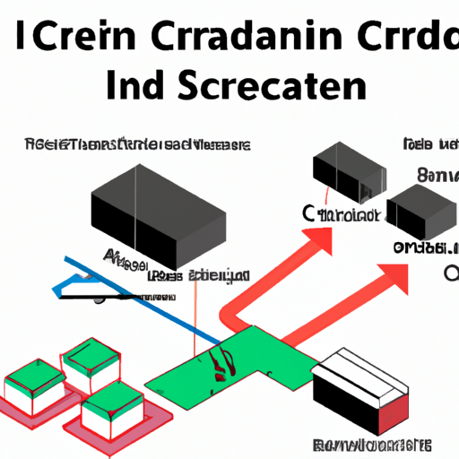
Title: The Mainstream Integrated Circuit (IC) Production Process: A Comprehensive Overview
1. Design and Layout (200 words) The IC production process begins with the design and layout phase, where engineers conceptualize the circuit's functionality and structure. Using computer-aided design (CAD) software, they create a detailed layout of the circuit, specifying the placement and interconnections of transistors, resistors, capacitors, and other components. This stage involves meticulous planning to optimize performance, minimize power consumption, and ensure manufacturability.
2. Photolithography (250 words) Photolithography is a critical step in IC production that involves transferring the circuit design onto a silicon wafer. A photosensitive material, called a photoresist, is applied to the wafer's surface. Then, a photomask, containing the circuit pattern, is aligned and exposed to ultraviolet light. The light passes through the transparent regions of the mask, exposing the photoresist in corresponding areas. Subsequently, the wafer is chemically treated to remove either the exposed or unexposed photoresist, leaving behind a patterned layer.
3. Etching (200 words) Etching is employed to remove unwanted material from the wafer's surface, following the pattern defined by the photoresist. Two primary etching techniques are used: wet etching and dry etching. Wet etching involves immersing the wafer in a chemical solution that selectively dissolves the exposed material. Dry etching, on the other hand, employs plasma to remove the unwanted material. Both techniques are crucial for creating the intricate structures and features of the IC.
4. Deposition (200 words) Deposition is the process of adding thin layers of material onto the wafer's surface. It is used to create conductive, insulating, or semiconducting layers required for the IC's functionality. Chemical vapor deposition (CVD) and physical vapor deposition (PVD) are the two primary deposition techniques employed. CVD involves introducing gaseous precursors into a chamber, where they react and deposit a thin film on the wafer. PVD, on the other hand, involves evaporating or sputtering a material onto the wafer's surface.
5. Doping and Diffusion (250 words) Doping is a crucial step in IC production that modifies the electrical properties of specific regions on the wafer. By introducing impurities, such as boron or phosphorus, into the silicon crystal lattice, the conductivity of the material can be altered. Diffusion is then employed to spread the dopants evenly throughout the wafer, creating the desired electrical characteristics. This process is essential for creating transistors, diodes, and other semiconductor devices.
6. Metallization and Interconnection (250 words) Metallization involves depositing a layer of metal, typically aluminum or copper, onto the wafer's surface. This layer serves as the interconnects, connecting various components of the IC. The metal layer is patterned using photolithography and etching techniques, creating the intricate network of interconnections required for the circuit's functionality. This stage is crucial for ensuring proper signal propagation and minimizing resistance.
7. Testing and Packaging (200 words) After the ICs are fabricated, they undergo rigorous testing to ensure their functionality and performance. Various electrical tests are conducted to verify the circuit's behavior under different conditions. Once the ICs pass the testing phase, they are packaged to protect them from external influences and facilitate their integration into electronic devices. Packaging involves encapsulating the IC in a protective material, such as plastic or ceramic, and connecting it to external pins or leads.
Conclusion (100 words) The mainstream IC production process is a complex and intricate series of steps that transform raw materials into highly sophisticated electronic components. From design and layout to testing and packaging, each stage plays a crucial role in ensuring the functionality, performance, and reliability of the ICs. As technology advances, the IC production process continues to evolve, enabling the development of smaller, faster, and more efficient electronic devices that have become an integral part of our daily lives.